

Diode Laser Tutorial - A comprehensive technical explanation of laser technology
Semiconductor diode lasers having sufficient power output to be useful in optical microscopy are now available from a host of manufacturers. In general these devices operate in the infrared region, but newer diode lasers operating at a variety of specific visible wavelengths are rapidly being developed. Diode lasers coupled to internal optical systems that improve beam shape and stability are now able to rival helium-neon lasers in many fluorescence microscopy applications. This interactive tutorial explores the properties of typical diode lasers and how specialized anamorphic prisms can be utilized for beam expansion.
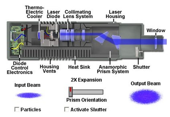
The tutorial initializes by displaying a blue diode laser in full operation and coupled to an Anamorphic Prism System set with an orientation that yields a 2x beam expansion. Light from the Laser Diode first passes through a three-element Collimating Lens System before entering a window and the first prism. In order to operate the tutorial, use the Prism Orientation slider to alter the relative position of the two anamorphic prism elements, subsequently modifying the degree of laser beam expansion between a range of 2x and 6x. The size and shape of the corresponding input and output beams are displayed in the lower portion of the tutorial window, and are modified as the slider is translated. The beam can be halted before exiting the laser housing by placing a checkmark in the Activate Shutter check box. Upon initialization, the tutorial displays the diode laser beam as a solid blue line that changes width upon translation of the Prism Orientation slider. The beam will be altered to simulate particles when the Particles check box is activated.
Diode lasers are fabricated utilizing a specialized type of semiconductor junction, and therefore share many of the advantages and characteristics of other semiconductors and solid-state devices. Although these lasers rely on electronic processes that take place in a solid semiconductor medium, the basic principles of laser action in diode lasers are no different from those controlling the operation of other (non-semiconductor) laser systems. In all lasers, it is necessary for energy transitions to occur among electrons in the lasing medium, and some of these must involve the emission of photons (categorized as optical transitions). In order for these transitions to result in emission of amplified light, the process of stimulated emission must predominate over either spontaneous emission or absorption. This situation is achieved under the conditions of a population inversion in the active medium, a process whereby the electron population of an upper energy level is induced to grow larger than that of a lower level.
In non-semiconductor lasers, which typically employ a single gas or gas mixture as the active laser medium, electron energy transitions occur within populations of individual atoms or molecules to produce the required population inversions. For semiconductor materials utilized for diode lasers, the flow of electrons within the crystalline solid must take place in a specific and predictable manner in order to produce a functioning laser. A single crystal semiconductor behaves in many respects as a large extended molecule, and its electronic and vibrational motions occur at discrete energy levels predicted by quantum theory. The energy levels of individual atoms and molecules in a gaseous laser medium can vary significantly in relatively large steps. However, in a crystalline solid, a very large number of electron levels occur that differ very little in energy or in quantum number.
In general, the energies of individual levels tend to group together into nearly continuous energy bands, the lowest of which is the fully occupied (filled) band that is made up of the inner electrons of the crystal's atoms. These tightly bound electrons do not take part in the bonding among constituent atoms of the solid. Instead, the bonding role is undertaken by electrons residing in the valence band, which consists of electrons at higher energy levels that interact in pairs to form somewhat-localized bonds between the atoms of the solid. Another band, termed the conduction band, also exists in the solid state at a still-higher energy level. Conduction band electrons are similar in energy to electrons that have been elevated to an excited state in individual atoms or molecules, and these have a high degree of freedom to move about within the solid. The difference in energy between the valence and conduction bands is defined as the band gap for a particular material. Energy relationships of the bands in different types of materials, including insulators, semiconductors, and conductors, are presented in Figure 1. The band gap energy is represented by the variable E(g), while kT is the thermal excitation energy and E(f) is the Fermi energy.
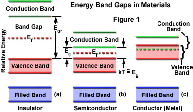
The range in magnitude of the band gap is critical to understanding the nature of electron conduction in semiconductors. In order for a solid to conduct electricity, its resistance must be low enough for electrons to move more or less freely throughout the bulk of the material. In insulators, the valence band is fully occupied and the only means by which an electron can move from atom to atom is for a valence electron to be displaced into the conduction band, which requires a substantial expenditure of energy. This behavior is consistent with the high resistance to electrical flow in insulators. Conductors, such as many of the common metals, have valence and conductance bands that partially overlap in energy (see Figure 1), such that a subset of the electrons from the valence band actually reside in the conductance band. The band gap is essentially zero for these materials, and with some of the valence electrons moving freely into the conductance band, vacancies or holes occur in the valence band. Electrons move, with very little energy input, into holes that occupy bands of adjacent atoms, and the holes migrate freely in the opposite direction. The movement of electrons and holes throughout the solid is the mechanism by which current is carried.
Semiconductors have electrical resistance values that are intermediate between those of insulators and conductors because these materials have band gaps that are small, but finite (as illustrated in Figure 1). Normal thermal agitation is sufficient to move a small number of electrons into the conduction band, and resistance can be reduced by increasing the temperature. Many semiconductor devices are designed so that application of a voltage produces the change in equilibrium electron population distribution that is necessary for current flow.
The simplest and most commonly utilized semiconductor is silicon, where each atom in the solid form shares electrons with four neighbors in a tetrahedral symmetry. Silicon is the example most often employed to illustrate various properties of semiconductors, although many important materials in diode laser applications are compounds of groups III and V elements, including gallium arsenide, indium phosphide, and indium arsenide. Even though the band arrangement is similar for all semiconductors, there are large differences in the band gap and in the distribution of electrons among the bands at specific temperature conditions.
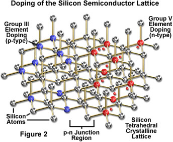
Pure silicon does not have a sufficient number of charge carriers under ambient conditions to be practical for devices such as the diode laser. However, the properties of silicon, as well as those of other semiconductor materials, can be modified during synthesis by the introduction of varying amounts of impurities into the crystalline lattice, a process known as doping (see Figure 2). Using the silicon lattice as an example in Figure 2, introduction of a small amount of a group III element results in an electron deficit, or electron hole (the blue atoms), in the crystalline lattice when compared to the normal electron sharing arrangement in pure silicon. In contrast, addition of a group V element as a dopant (the red atoms in Figure 2) produces an excess electron that is not a shared member of the lattice, and therefore is mobile within the structure. Semiconductor materials that are modified, or doped, in this manner are termed n-type semiconductors if they have excess electrons, and p-type semiconductors if they contain excess holes.
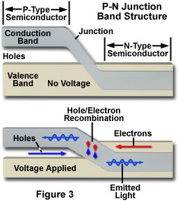
At the junction between regions of p-type and n-type semiconductor materials, an unusual set of electronic conditions exists that comprises the basis for all semiconductor-based devices, including the diode laser. When these two types of semiconductor materials are closely joined, any shift of the equilibrium distribution among energy levels can cause a current to flow across the p-n junction (see Figures 2 and 3). In semiconductor devices, a voltage applied to the junction provides a shift in the Fermi level (the deviation from statistical, or Boltzmann, electron population distribution) on opposite sides of the junction, and electrons move toward the p-type region, while holes simultaneously flow into the n-type region. In some cases, the system can relax back to the equilibrium electron distribution through the emission of a photon by the spontaneous emission process. The band gap of the material determines the energy of the emitted photon. Emission of light resulting from the recombination of electrons and holes in the p-n junction region is the underlying mechanism of the light emitting diode (LED), which is directly related to diode laser function. Illustrated in Figure 3 is a representation of the band structure from a typical p-n semiconductor junction.
As discussed previously, if electron transitions in a material can be induced to produce a population inversion, and the consequent statistically higher probability of stimulated emission, then a net light amplification results. In a typical laser, the light produced is confined to the active medium, and opposing mirrors are utilized to produce multiple reflections within the medium in order to increase the gain in light output from the laser cavity. One of the mirrors is designed to totally reflect light back into the cavity, while the other is able to transmit a portion of the amplified light as the output beam. This simple scheme is the primary basis for laser function.
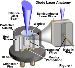
At the junction between p-type and n-type semiconductors, a population inversion can be created among the energy levels of electrons and holes if sufficient electrical energy is applied to the junction. With the dominance of stimulated emission that results from a population inversion, the only remaining requirement for laser action is to confine emission so that it is directed primarily along the junction boundaries, and undergoes amplification or gain before being emitted from the semiconductor material. In diode laser devices, confinement of emitted light to the optical cavity is often achieved by applying reflective coatings to opposite ends of the laser crystal. However, in some cases, even this simple step is not required. Because the refractive index of most semiconductor materials is significantly higher than that of air, sufficient internal reflection occurs at the boundaries of the crystal to confine the emission and sustain laser action in many laser materials. Figure 4 illustrates the structure of a simple gallium arsenide diode laser.
Most diode lasers are based on crystal wafers of group III-V compounds from the periodic chart of elements. Those fabricated from gallium arsenide and its derivatives typically lase at wavelengths between 660 and 900 nanometers, and those utilizing indium phosphide-based compounds produce wavelengths between 1300 and 1550 nanometers. The dominant segment of the market is the shorter-wavelength lasers, with the most common application being in digital optical signal storage and retrieval, such as compact disc audio systems and read/write devices. The longer-wavelength diode lasers are primarily used by the telecommunications industries for fiber optic data transmission. Diode lasers can respond very rapidly, and in a linear fashion, to changes in driving current, which is a significant advantage in telecommunications transmission. The capability of a light source to be modulated at extremely high rates enables an enormous number of signals to be carried on a single optical fiber.
As the technology surrounding the diode laser has evolved, dramatic improvements have been made in the efficiency, spectral characteristics, and functional lifetime of the devices. A primary objective in design of these lasers is preventing internal loss of radiation due to excessive beam spread from the small junction, where gain occurs. Through various techniques for confining the beam, not only is the efficiency and output power of the laser maximized, but also certain other characteristics of the beam are affected in a desirable manner.
Application of a specialized heterojunction (a junction between two different materials) is one mechanism by which the natural properties of the semiconductor junction are exploited to confine a laser beam. The most common heterojunction utilized in diode lasers is formed between gallium arsenide and gallium aluminum arsenide. Improvements in laser operation utilizing this design result from the fact that band gap differences between dissimilar materials serves to confine either electrons or holes to the junction region (increasing optical gain). Emitted light is also largely restricted to the region due to refractive index discontinuities of the heterojunction. The double-heterojunction is another advance that benefits from confinement of both charge carriers and photons to the active region, yielding further improvements in efficiency.
Although the junction properties and configuration can be manipulated to confine the diode laser beam to the plane of the junction, other modifications in wafer geometry are often employed to further restrict the beam. Numerous variations in diode architecture are applied to achieve specific operational goals, such as high power or bandwidth tuning, but two of the most basic mechanisms for beam spread control are gain-guiding and index-guiding. With the gain-guided design, utilized since the earliest diode lasers, photons are concentrated in the vicinity of the greatest charge carrier flux created in the junction, which is determined by the shape of the metallic electrode strip on the wafer surface. The index-guided design relies upon a waveguide groove that is formed in the wafer during the deposition process. The groove, adjacent to the active junction, creates a geometry that confines laser radiation on four sides by refractive index discontinuities. The index-guided laser has an additional advantage in that it reduces astigmatism of the output beam, an unfortunate feature of the diode laser that must be eliminated for many applications.
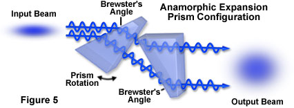
In spite of their numerous advantages, some of the output beam properties exhibited by diode lasers are not appropriate for specific applications, and must be corrected by addition of optical elements or other by mechanisms. The output of most diode lasers consists of a single transverse mode that is equivalent to the TEM(00) mode of conventional laser systems. The intensity profile in the transverse direction of the beam is pseudo-Gaussian, which is desirable for most laser applications in optical microscopy. However, the beam emitted from a typical diode laser is highly elliptical, and the specification of beam divergence as compared to that of a symmetrical Gaussian beam differs significantly. Figure 4, which outlines the basic structure of a diode laser, also illustrates the beam ellipticity upon emission from the output face of the active layer. The beam asymmetry results from the fact that a typical junction may have a thickness of only 0.1 micrometer, but may extend to 5 micrometers or greater in width. As a result, divergence in the plane parallel to the junction layer can be 5 or 6 times less than in the direction perpendicular to the layer. The collimated beam will exhibit divergence at a distance that is different in the two directions. If this beam asymmetry is important for a particular application, it can be corrected with specialized optical systems, such as anamorphic prisms, which function by expanding the minor axis of the output beam. The tutorial illustrates the placement and utilization of these prisms in the optical path of a typical diode laser system.
Beam astigmatism is another potential disadvantage of laser diodes, particularly in gain-guided designs. Because the beam dimension is defined by properties in the plane of the junction that differ from those in the plane perpendicular to the junction, the beam appears to diverge from different points when viewed from those two orthogonal directions. Index-guided lasers dramatically reduce astigmatism, but commercial laser diodes typically exhibit as much as 5 micrometers of uncorrected astigmatism. The easiest technique for correcting astigmatism is the introduction of a weak cylindrical lens. However, if complete removal of the aberration is necessary, the laser system should provide adjustable auxiliary lens components (such as a positive or negative lens to add or subtract power from the axes).
Low power diode lasers are typically manufactured in a package that includes a photodiode employed to monitor the laser output in order to act as a feedback power control. In addition, planar glass window usually seals the output end of the integrated package (see Figure 4). Spherical aberrations introduced by this window must be corrected in the design of the beam-modifying optics in order to achieve optimum performance.
The high divergence of diode lasers can be corrected by utilization of a high numerical aperture compound-element collimating lens, which can also be designed so that the first element of the lens system eliminates aberrations from the glass window. Commercially available diode laser systems often combine the laser diode and beam correction optics into a pre-aligned head assembly. In these designs, a weak cylindrical lens placed after the beam-collimation lens system can correct the beam astigmatism mentioned previously, and ensure that the beam's apparent point of origin is the same in both orthogonal planes.
Following collimation of the beam, in order to minimize far-field divergence, the elliptical cross-section must be transformed by expansion in one dimension to make it circular. An anamorphic prism pair, mounted as illustrated in the tutorial and Figure 5, can accomplish this expansion. Two identical prisms are mounted at an angle (approaching Brewster's angle) to the incident beam, which is then shifted by a small increment laterally, while being expanded in one direction (anamorphically). The magnitude of the expansion is determined by the angle between the two prisms. For optimum performance of a diode laser system, alignment tolerances are extremely small, usually on the order of micrometers. Interferometry is the only reliable method of carrying out the alignments and verifying the performance of the laser assembly. For this reason, most commercial assemblies combine all of the laser components in a rigid package that protects alignment and shields the optical components from dust.